
Product
Semiconductor test shape exposure
(e.g., 2D materials, photomask-free development, exposure units targeting photomask-free development needs)
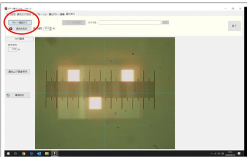
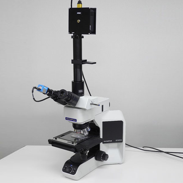
- The microscope LED exposure system (UTA series) is a projection-type exposure device that can perform shape exposure without the need for a photomask.
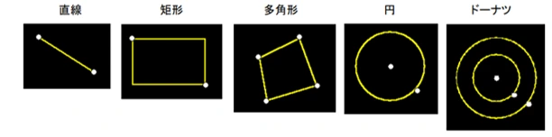
- Using a metal microscope and an LED light source DLP projector, correction can be performed under a microscope, allowing arbitrary shapes with a resolution of μm to be projected onto a substrate coated with photoresist for exposure.
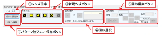
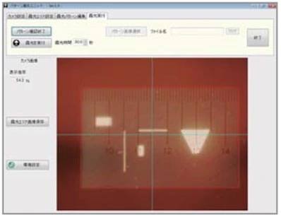
- The image to be exposed can be freely edited using dedicated software, and the completed image can be saved. Alternatively, it can also read externally created BMP files for exposure.
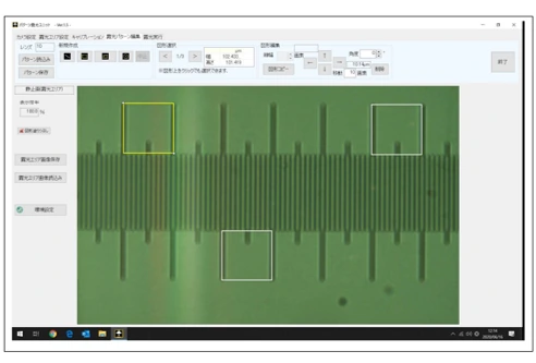
- This equipment can create the required electrode patterns on layered monocrystalline wafers of various sizes and shapes under atmospheric conditions. Therefore, it is cheaper and easier to use compared to electron beam lithography machines. In addition, it eliminates the need to use expensive electrode patterns to create photomasks for exposure.
<Application examples>
Electrode formation for samples used in thin-film FET or Hole effect measurement.
Electrode formation is performed when thin sheets extracted from graphene-molybdenum raw materials are used to evaluate the properties of the raw materials.
Exposure pattern creation for research and development.
<Features>
This device is a combination of a microscope and a DLP projector, making it cheaper than other exposure equipment currently available on the market.
The light source uses white LED light. Any exposure time can be set.
With user-friendly software, you can easily create the desired exposure patterns. → Includes positive and negative exposure conversion function (supports one-click).
It can read complex BMP files created by other software for irradiation.
Exposure is achieved through different objective lens magnifications, thus catering to everything from minute shapes to a wide range of exposure needs.
It can be installed on virtually any microscope (the specifications of the existing microscopes need to be checked for evaluation).
It can produce shapes with resolutions in the μm range.
Minimum linewidth approximately 1 μm (not guaranteed).
Exposure range: Objective lens 5X: approx. 1.85mm × 1.15mm / Objective lens 100X: approx. 90μm × 57μm
※The above are reference values for UTA-1AS-53M-SET.